- Home»
- An Introduction to Our Technology»
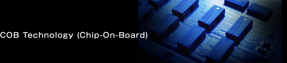
- COB Technology (Chip-On-Board)
Features
- Based on its wealth of experience in the plating industry and the strict product quality management of its technical professionals, Satosen is proud to present its highly-trustworthy and stable COB technology. For over the last twenty years, Satosen has put together an unrivalled record when it comes to everything from development to mass production of COB.
- Even in cases where, for design reasons, tie bar can't be used for electrolytic bondable gold plating, using its proprietary methods, Satosen is able to carry out tie bar less electrolytic bondable gold plating.
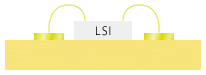
- With its ability to produce spot-facing (cavities) for IC mounting, Satosen is able to embed built-in LSI.
Equipped with a sensor for detecting board thickness, Satosen’s routers are used to realize high-precision spot facing.

- Satosen maintains bonding machines and pullcut testers in-house, giving it a quality assurance structure in the form of the various types of solution analysis, SEM and the like.
Various Types of Surface Treatment
- Having its roots in the plating industry, Satosen provides surface treatments with unparalleled component bonding strength.
- Electrolytic bondable gold/silver plating (leadless gold plating is available)
- Non-electrolytic bondable silver plating
- Non-electrolytic bondable gold plating (leadless is available)
- NiPdAu bondable gold plating (bonding and soldering by means of non-electrolysis plating)

![]()