Happy Halloween!
It is getting colder and colder every day in Japan.You can easily get sick when the seasons change. Please take care of yourself.
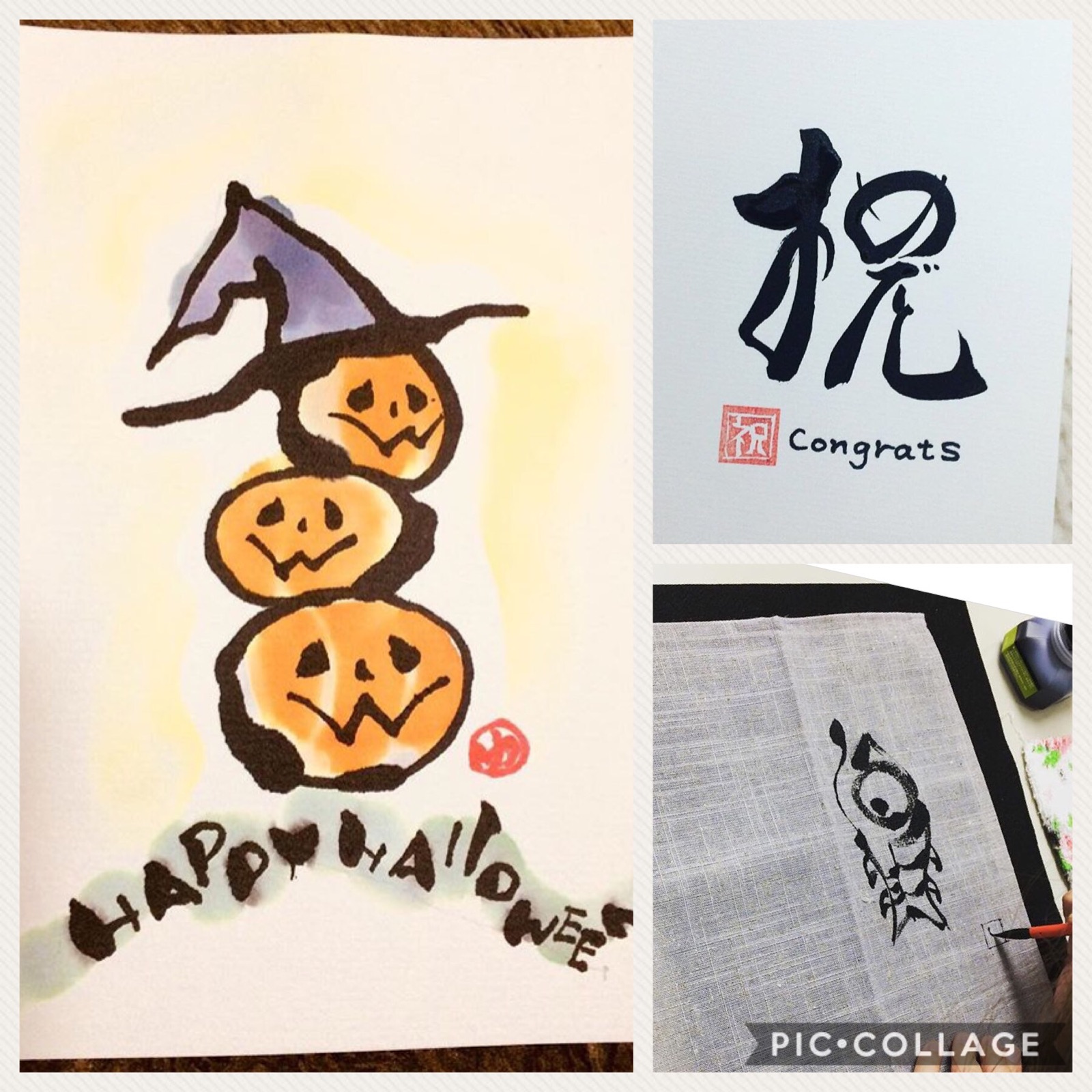
Recently, I have started taking up Japanese calligraphy class as a hobby. We can learn not noly calligraphy but also painting in this class.
This is a picture with Halloween as a theme using calligraphy.
It is really fun. Please try Japanese calliraphy, if you have a chance.
Nanobondα
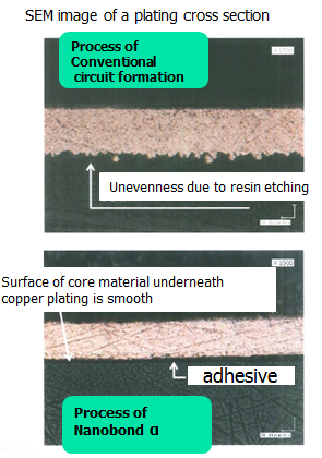
It enables to make plating on various material surface.It is the way of making image with the ink directly follow by plating . It is very simplified and short process only.
It is also friendly to the material surface because of no etching process required.
Interface between plating and the material is very smother than that of conventional method. (Plese refer to the difference in photo at right. So it is popular to use for precise sensing device and technologies and also antenna for RFID application etc.
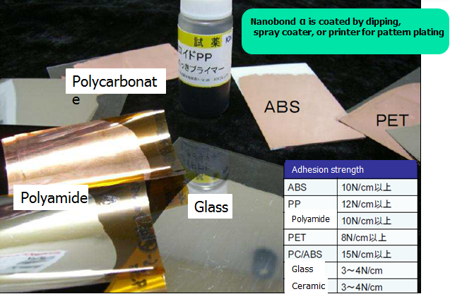
Above is pull strength of copper on each material.We recently suceed to make plating on PPS and COP and confirmed the stregth was 5N and 3N.Although we can not disclose at this moment, envolved latest technology is also present with this.We hope we can introduce in face to face.
If you have any enquiries/RFQ please feel free to contact with us.